With the increasing importance of hyperspectral and multispectral imaging, as we commented in one of our previous articles, the use of cameras in spectroscopic applications has also grown. In this post we will describe the operation of a scientific camera as well as the main existing types (silicon-based CCDs, CMOS sensors and InGaAs sensors), including their advantages and disadvantages.
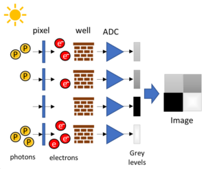
The process by which a camera generates an image after being exposed to a light source consists of the following steps (see Figure 1):
1. Photons are detected by cameras thanks to the use of photodetectors. These photons are converted in an equivalent number of electrons. The efficiency of this conversion (% of photons that convert into electrons) is called quantum efficiency.
2. The photodetector is divided in small squares called pixels. Each pixel has an associated well that stores the electrons generated by the photons hitting that pixel. For a photodetector of a given area, the higher the number of pixels, the higher the resolution but the lower the sensitivity (as each pixel has a lower area). Therefore, a trade-off between resolution and sensitivity is required.
3. The number of electrons per well (per pixel) is then converted from a voltage into a digital signal by employing an analogue to digital converter (ADC).
4. These digital signals are converted into grayscale colors known as gray levels. The higher the level, the brighter; and the lower the level, the darker. The number of gray levels depends on the dynamic range of the sensor.
5. An image, that consists of the grey levels associated to each pixel, is obtained at the end of this process..

Depending of the wavelength of the photons that we want to detect, the photodetectors must be made of a different material, which leads to many different kinds of camera technologies:
- Silicon-based CCDs: CCD stands for charged-coupled device. They consist of a silicon surface onto which an integrated circuit is etched, creating an array of pixels. The electrons generated by the photons that hit each pixel are shifted along the sensor to readout registers where they are converted into grey levels. Silicon-based CCD cameras are suitable for the UV-VIS-NIR range, but they are not sensitive enough for wavelengths higher than 1100 nm.
- CMOS sensors: CMOS stands for complementary metal-oxide-semiconductor. Their main difference with CCD sensors is that instead of having a single ADC for all the pixels, they have a capacitor and amplifier for every pixel and an ADC for every column of pixels, see Figure 2. This makes the readout process of the whole sensor much faster (up to 5 times). In addition to this, CCD sensors consume less power (around 100 times) and have lower noise. CMOS sensors work more or less in the same wavelength region as CCD cameras.

- InGaAs sensors: they consist of an InP (indium phosphide) substrate, an InGaAs (indium gallium arsenide) absorption layer under it and an ultrathin InP cap layer. This last layer is connected through indium bumps to a readout integrated circuit. InGaAs sensors are suitable for the SWIR range, from 900 to 1700 nm, although some sensors can measure up to 2500 nm thanks to changes in the material composition. The worse problem present in InGaAs sensors is the noise level, in particular, the dark current noise, which is associated to the thermally generated electrons. The solution consists in cooling the camera.
These cameras can be combined with broadband light sources (as our TAKHI Halogen light source) for hyperspectral and multispectral imaging applications such as agriculture (monitoring of the development and health of the crops), food processing (sorting, identification of foreign bodies, quality evaluation), medicine (non-invasive scans of the skin) or geology (identification of minerals).
Written by J.J. Imas
Bibliography
Fundamentals behind modern scientific cameras. Educational notes.
Scientific CMOS (sCMOS) Cameras: The Basics.
Silicon-based CCDs: The Basics. Educational Notes.
InGaAs Cameras: The Basics. Educational Notes.
